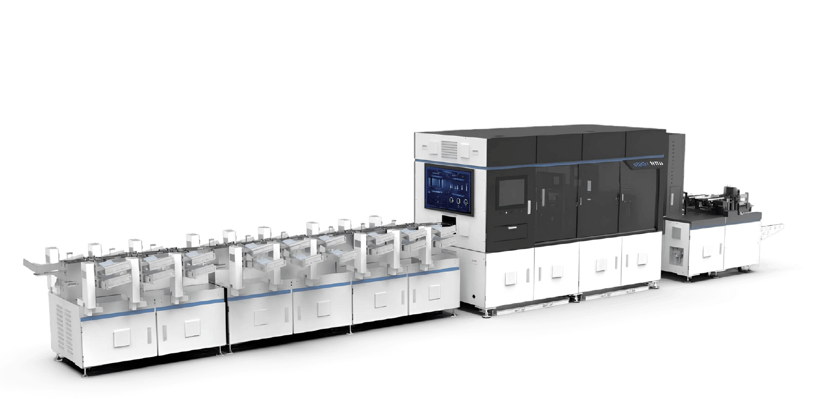
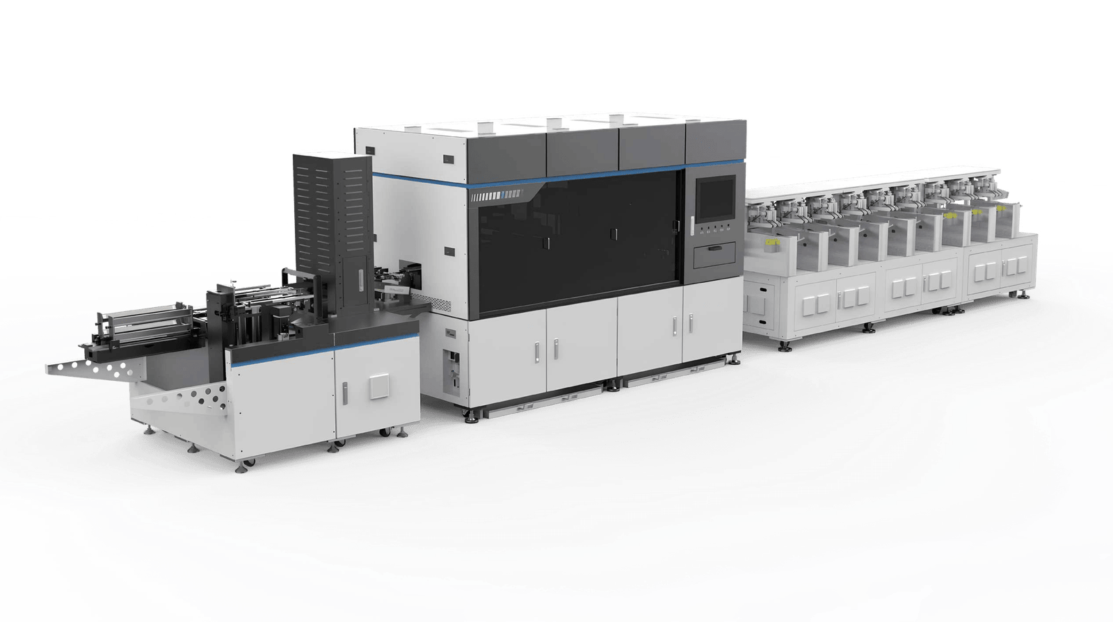
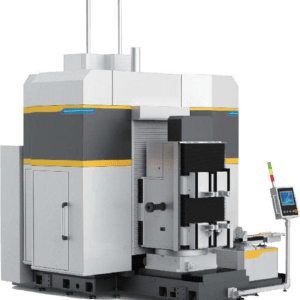
Our Wafer Inspection and Sorting Solution is designed to deliver high-speed, high-precision, and high-capacity inspection for modern wafer manufacturing. By combining advanced imaging technology, intelligent algorithms, and automated handling, the system ensures reliable quality control while maximizing production efficiency and reducing manual intervention.
The system features a dual-station design that enables continuous wafer loading and unloading, minimizing idle time and supporting uninterrupted production. This configuration integrates seamlessly with automated manufacturing lines, improving throughput and enhancing the overall efficiency of the production process.
Advanced optical inspection technology accurately detects wafer defects, including wafer fragments, chips, cracks, and other surface imperfections. High-speed image acquisition and precise inspection capabilities ensure that only qualified wafers proceed to the next production stage, helping to improve product yield and maintain consistent quality standards.
At the core of the system is a self-developed algorithm platform that combines artificial intelligence (AI) with traditional image processing algorithms. This hybrid approach significantly improves detection accuracy while reducing false detections. The platform also provides configurable inspection parameters, allowing users to customize inspection criteria according to specific production requirements and optimize performance for different wafer types and manufacturing processes.
With its combination of intelligent inspection, automated sorting, flexible configuration, and high production capacity, the Wafer Inspection and Sorting Solution provides a reliable, efficient, and future-ready quality control system for advanced semiconductor and photovoltaic manufacturing.